Technical Papers
Bonding Papers
Our technical papers provide in-depth insights into numerous challenges of today’s applications, technologies and processes and introduce you to proven solutions by Finetech.
Indium Bump Interconnect (IBI) Flip Chip Bonding
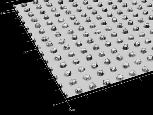
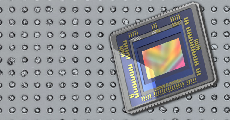
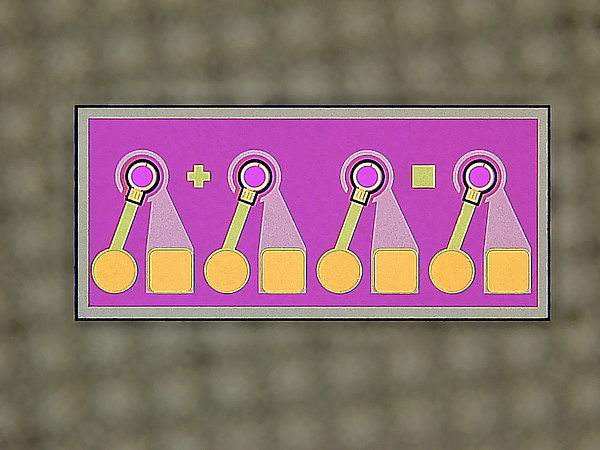
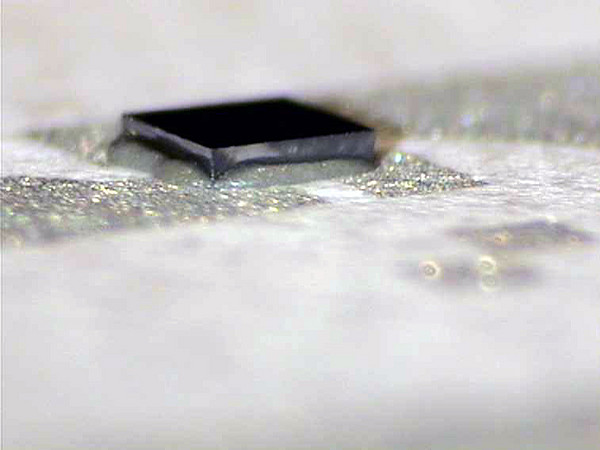
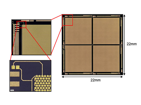
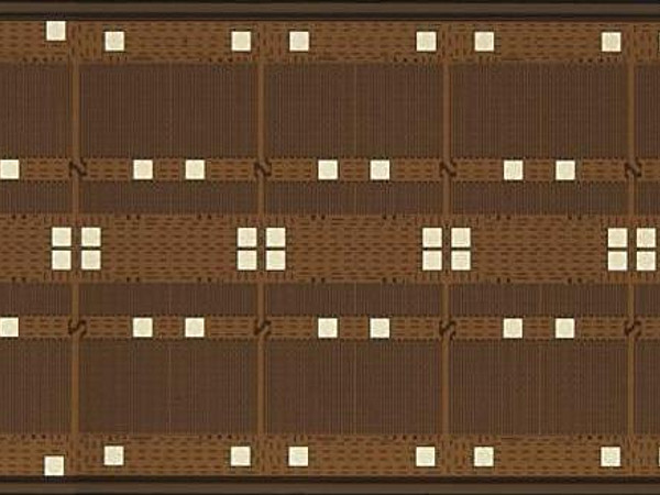
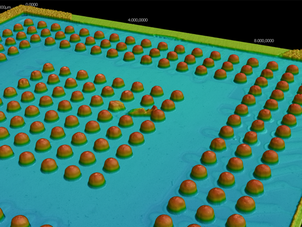
Higher pixel / Qubit count and interconnect density on larger and larger chips is driving hybridization and monolithic integration. This results in increased demand for fine pitch micro Indium Bump Interconnect (IBI) flip chip die bonding solutions.
IR Sensor Bonding
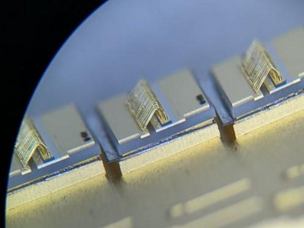
The preferred way of hybridization to produce large format, high density infrared (IR) thermal imaging sensors according to industry requirements is by using fine pitch micro Indium bump array interconnect bonding. However, there are specific challenges associated with Indium bump-to-bump die bonding.
Automated High Power Laser Diode Assembly
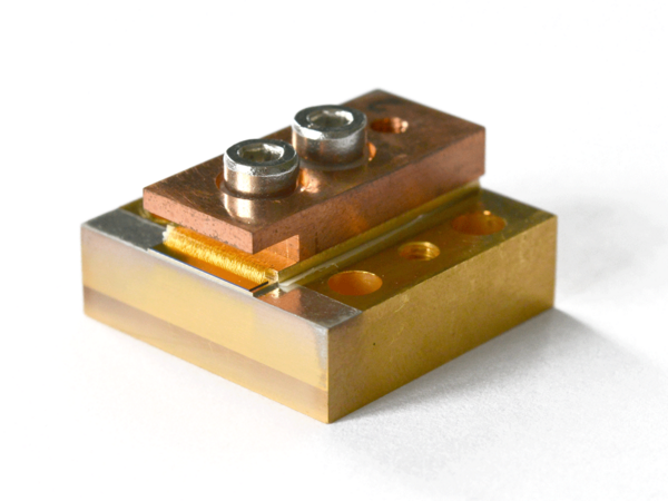
High power laser diode assembly is a mass production process. An automated laser diode bonder is expected to output complete assemblies at a high unit/hour rate, while maintaining high accuracy and high repeatability for maximum yield over a large variation in component size, and type.
Prototype-to-Production
Finetech's "Prototype-to-Production" approach enables fast, creative and flexible product development and seamless process transfer from R&D to production, saving you time and minimizing technological and financial risks.
How we understand accuracy
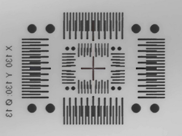
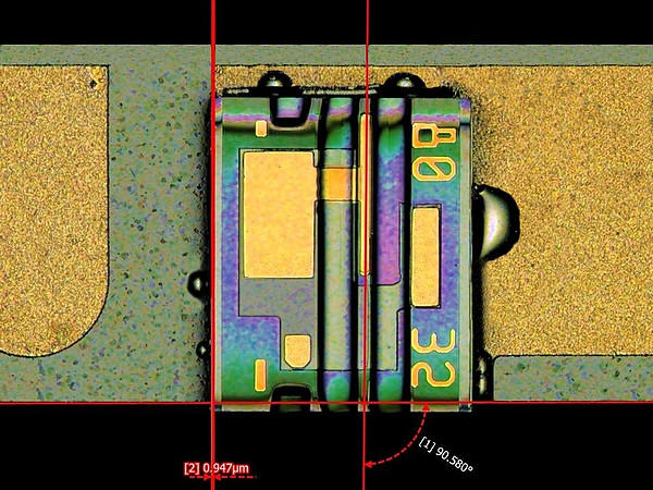
This paper provides a transparent and verifiable method description of how the accuracy of Finetech placement and assembly systems is measured and specified.
Laser Bar Bonding
Semiconductor Laser diode bars are high power products, used in places where small and efficient emitting light sources are needed. Primarily, these Lasers are being used as pumping sources for optical resonators of solid state Lasers or gas Lasers.
Optical Package Assembly
Optical packages are assemblies comprising optical and electronic components. Applications can be found e.g. in communication technologies where optical signals are transformed into electrical signals and vice versa.
VCSEL Assembly
The packaging of opto-electronic units is one of the key applications of Micro Assembly. Highly dense packaged multiplex transmitters, receivers and combined assemblies are...
Eutectic Bonding with Au/Sn
Eutectic Gold/Tin (Au/Sn) is a hard solder alloy often used to bond demanding microelectronic and optoelectronic devices. They are available in different forms, such as pre-forms, solder paste or ribbons.
Multi Emitter Module Assembly
In order to reduce second-level packaging costs for optoelectronics manufacturing, Finetech has evaluated and is now offering an automatic solution for the packaging of CoS onto a heat sink via reactive multilayer systems (RMS).
Bonding with Anisotropic Adhesive
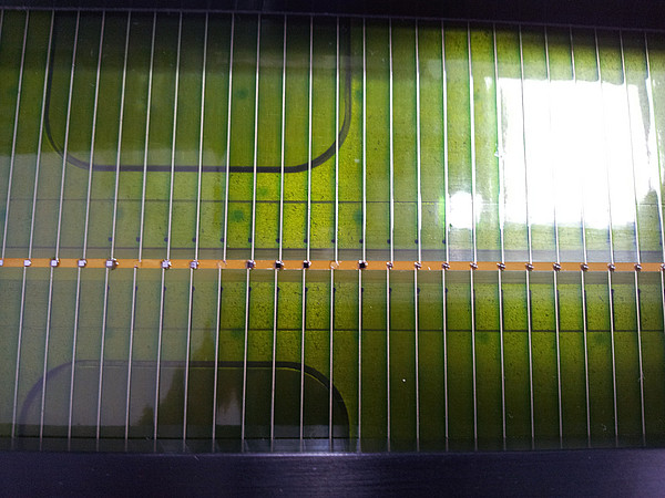
In modern displays, Flex-on-glass and Chip-on-Glass are preferred bonding technologies. This goes along with using anisotropic conductive foils or pastes which have a fundamentally different functional principle compared to common adhesives or solder materials.
Laser Assisted Die Bonding
Finetech's laser-assisted bonding technology is used in C2S and C2W applications with high demands regarding speed, highest accuracy and localized heat input.
Thermocompression Bonding
Thermocompression bonding is a quick and easy method to reliably connect flip-chips. As the name suggests, this connecting method relies on force and temperature.
Focal Plane Array (FPA)
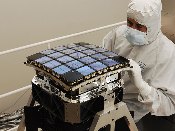
A Focal Plane Array (FPA) is a sensor with a two-dimensional detector pixel matrix, i.e. for infra-red light or X-rays, positioned in the focal plane of an optical system.
RFID Assembly
RFID chips (Radio Frequency Identification) are increasingly used in industrial and consumer products. They come in sizes from several millimeters down to a few microns, with very thin and flexible substrates prone to thermal stress.
Adhesive Technologies
Between two bond partners, adhesive materials can be applied in various ways: dispensing, stencil printing, pin transfer or as a film working as an intermediate connection.
Ultrasonic Die Bonding
Ultrasonic / thermosonic bonding is a process primarily used for bond wires but also for flip chip bonding. Ultrasonic allows to generate a mechanically and electrically stable connection.
Bonding Technologies for 3D Integration
An overview about different interconnects used during the system evaluation of the FINEPLACER® sigma
Flip-chip Bonding to Organic Substrates
Standard IC packages with an increased number of I/O pads suffer from larger volume, increased cost, increased wire bonding resistances and parasitic inductances while offering...
Rework Papers
Our technical papers provide in-depth insights into numerous challenges of today’s applications, technologies and processes and introduce you to proven solutions by Finetech.
Checklist - Which rework system fits your requirement profile?
This checklist helps you selecting a professional SMD rework system that suits your individual requirements.
Rework of 01005 and 008004 Small Passives
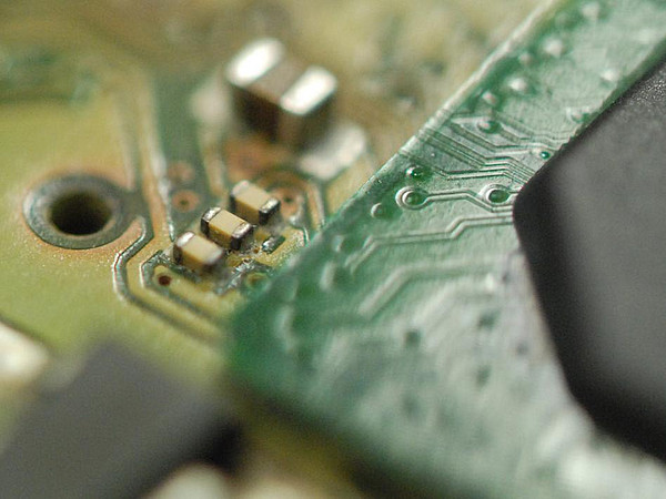
008004 and 01005 small passive components are becoming more and more important these days (integration, miniaturization etc.). They allow particularly flat package designs when developing ultra-mobile electronic products such as functional modules,...
Rework of Mini-LED Arrays
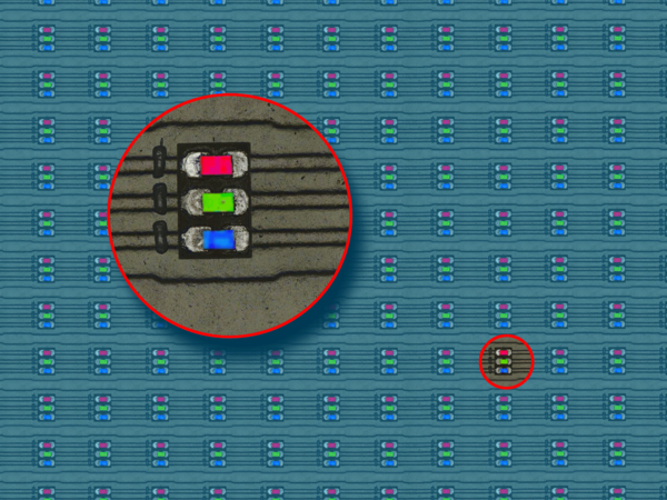
Finetech rework systems for R&D and production environments are well suitable for miniature LED rework, such as those in form of SMD LED components (RGB) built into modern display systems.
Array Reballing
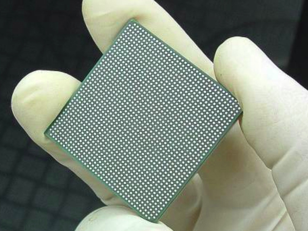
Precise placement of a new solder ball array is called array reballing. This repair process is applied when saving valuable resources (and money) is crucial or when the value chain has to be extended.
Rework of Shielded SMD
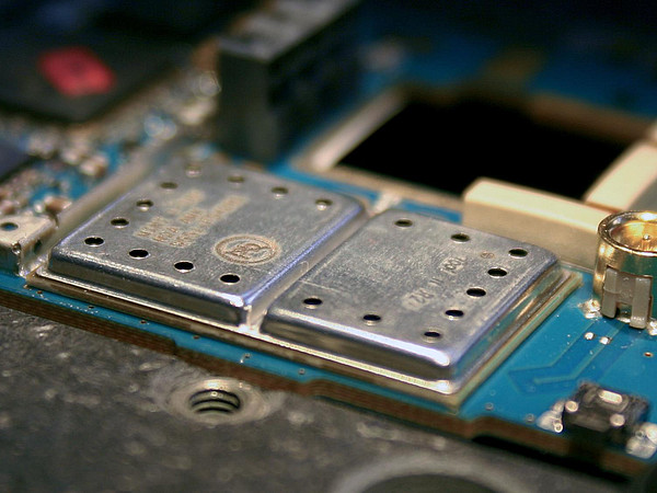
As the PCB market continues to be in high demand, the RF shield design will remain a challenge to rework. Simply put, the RF shield serves one goal – to minimize the Radio Frequency (RF) noise which can...
Residual Solder Removal
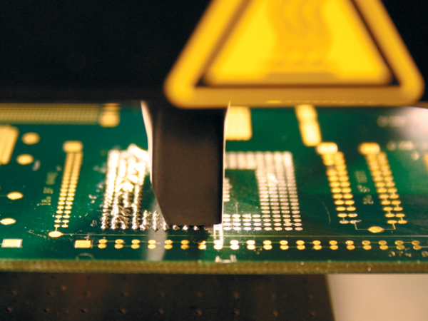
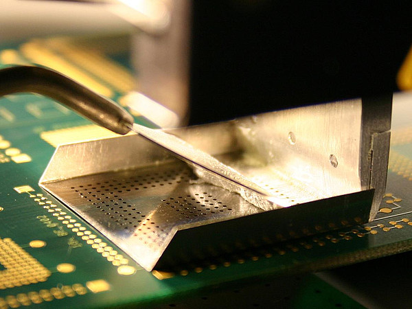
An accurate residual solder removal is an essential factor of success for most rework applications. Finetech offers contactless removal solutions for virtually all SMD components in the market.
Applying Solder Paste
Finetech offers a variety of equipment solutions for suitable solder paste application during the rework cycle.
Package on Package Rework (POP)
Package-on-package (PoP) is an electronic circuit consisting of superposed, electrically connected assemblies. The lower module, which is the logic component, is commonly called bottom package, on top of which usually the top package module is situated.
Rework on Flex Materials
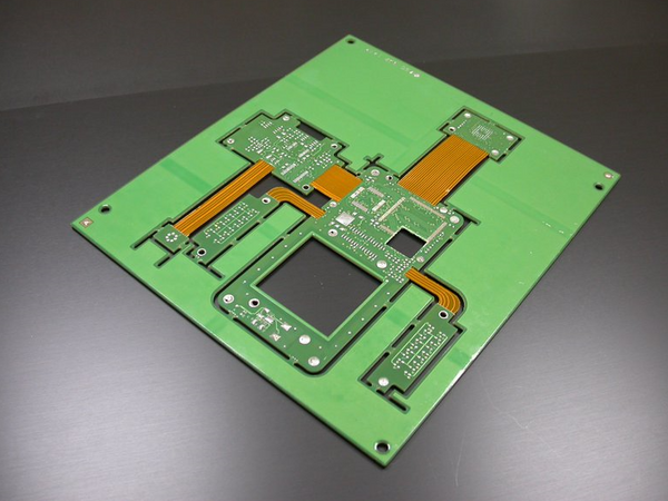
Flexible substrates are used in 3D connection and mechatronic concepts for reducing the number of connectors needed. They can stand high dynamic bending and are capable of high speed interconnections between
Rework of BGA/CSP and CPU/GPU SMD
The rework of BGA components with large ball arrays, processor units (CPU) as well as graphics chips (GPU) and CSP with a fine pitch array demand special device configurations that combine precise thermal management with high placement accuracy and high-resolution optics.
Flip-Chip rework
Flip chip components have rarely been used in PCB assembly, but they are becoming more and more important as the need for miniaturization of electronic assemblies is growing.
Rework of QFN/MLF
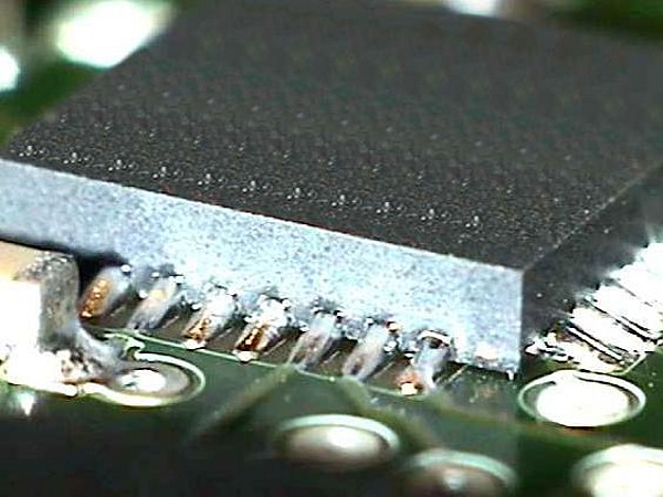
Flat packages such as QFNs (Quad Flat No-lead) or other MLFs (Micro Lead Frame) with outstanding thermal, inductive and capacitive characteristics (for example resulting in much shorter reaction times) are being increasingly incorporated into...
Rework of SMD Connectors
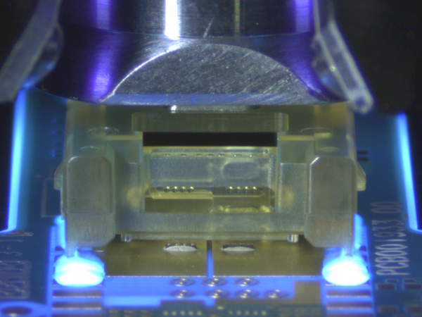
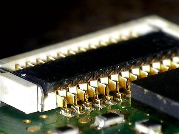
Due to their reduced space requirements, miniaturized SMD connectors are increasingly being used for small component assemblies, for example, found in mobile devices. Large SMD connectors and plugs are also widely spread.
Single Ball Reballing
One defect solder ball is enough to render the complete BGA package unusable. The capability to replace single solder balls allows to save particularly valuable or legacy packages.
Rework of Underfilled SMD
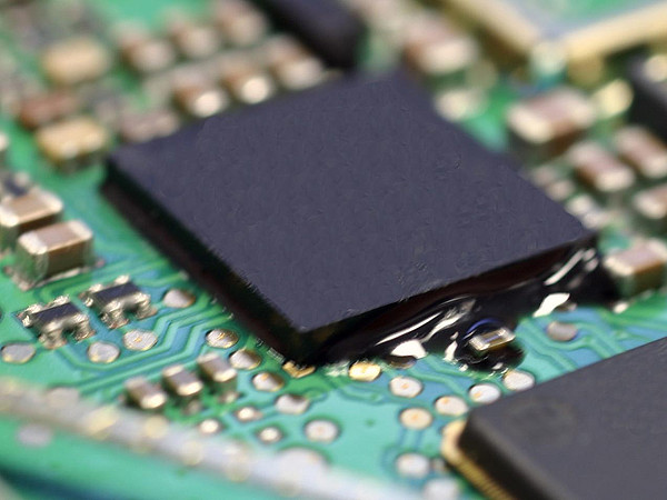
Underfilled components are used in consumer electronic products (mobile devices, portable computers etc.), in the automotive industry (sensor modules, engine control units etc.) or whenever flip chips are incorporated in...

