
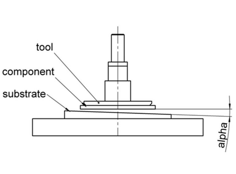
// Coplanarity in Bonding
During the IMAPS Conference and Exhibit in San Diego last month, one of the topics mentioned over and over again was coplanarity in die bonding.
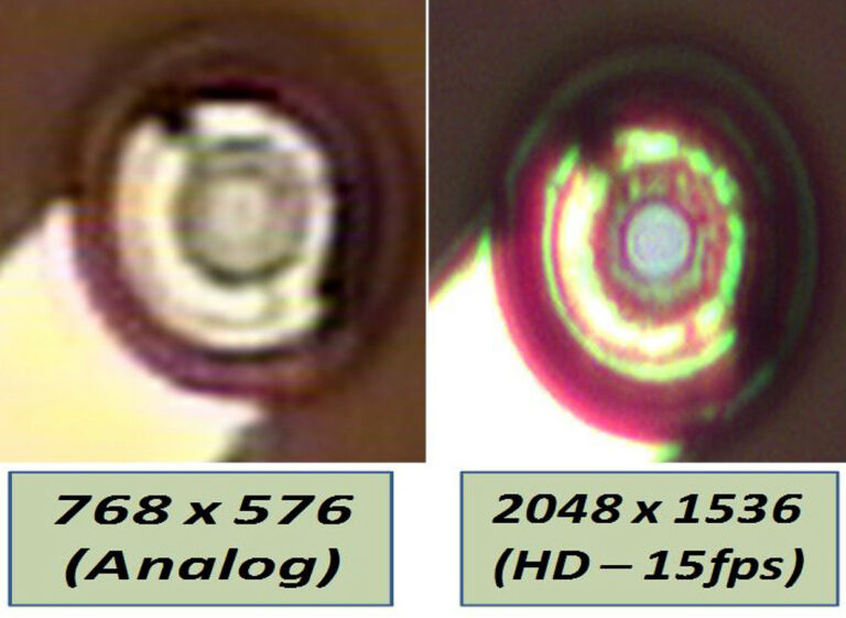
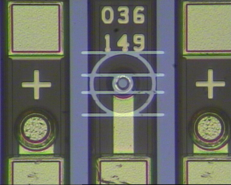
// Optical Resolution for Bonding
High accuracy die placement requires precise magnification and resolution. It is nearly impossible to achieve sub-micron placement without accurate use of both of these elements.
// ACF / ACP Bonding
Using tiny polymer spheres coated with gold will allow an electrical connection to be made between a die and substrate.
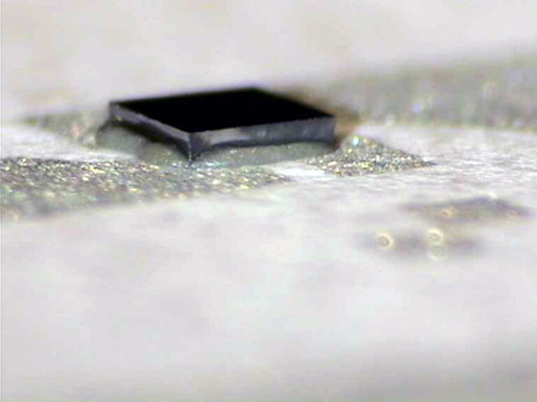
// Thermosonic Bonding: Small Die
In my last blog I wrote about the challenges involved with thermo-sonic bonding of large die. Thermo-sonic bonding of smaller die presents…
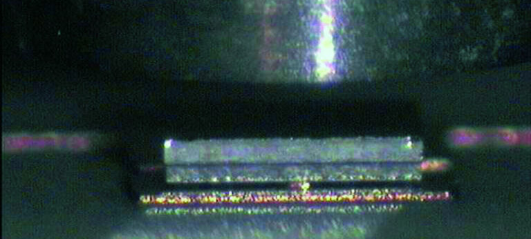
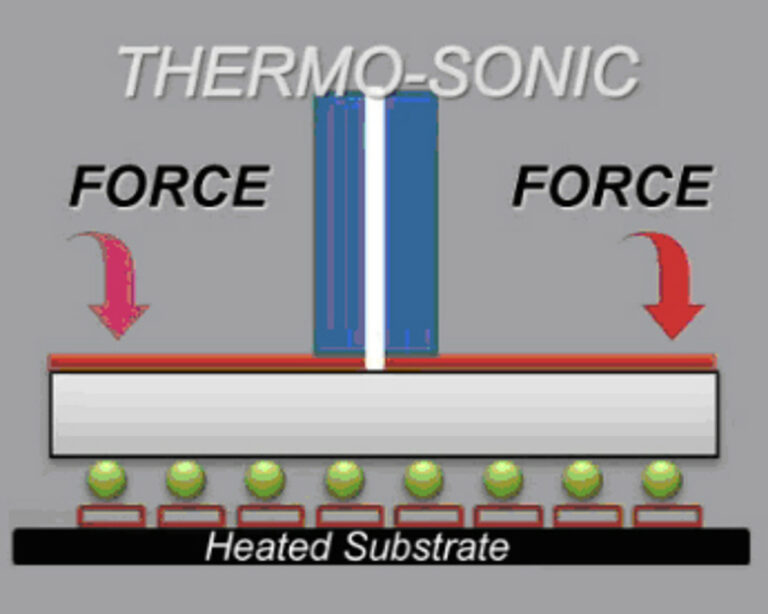
// Thermosonic Bonding: Large Die to Substrate
Thermo-sonic bonding is the process of flip chip bonding a die to a substrate using gold as the interconnect while avoiding high temperatures.
// VCSEL and Photo Diode Alignment Simplified
Aligning a 4-channel VCSEL and a 4-channel photo diode together on a PCB, using conductive epoxy, is a challenging application for most telecom companies that develop and manufacture VSR or
