How Finetech, together with First Sensor AG, developed a complete solution for reproducible rework of faulty photodiode arrays for CT detectors.
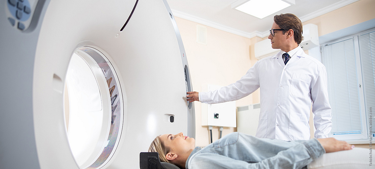
In the growing sensor market, First Sensor AG develops and produces standardized and customer-specific solutions for numerous applications. Based on proven technology platforms, a wide range of products are developed, from chips to components and detectors to sensor systems. Among other things, First Sensor is a strategic partner for leading medical device manufacturers in the field of medical diagnostics. Here, imaging procedures such as endoscopy, computed tomography (CT) scans and magnetic resonance imaging (MRI) play an important role in the identification of diseases and functional disorders and what causes them.
Problem Definition
Together with an end customer, First Sensor has developed the assembly and packaging technology for sensor modules used in computed tomography and also manufactures at the Berlin-Weißensee site.
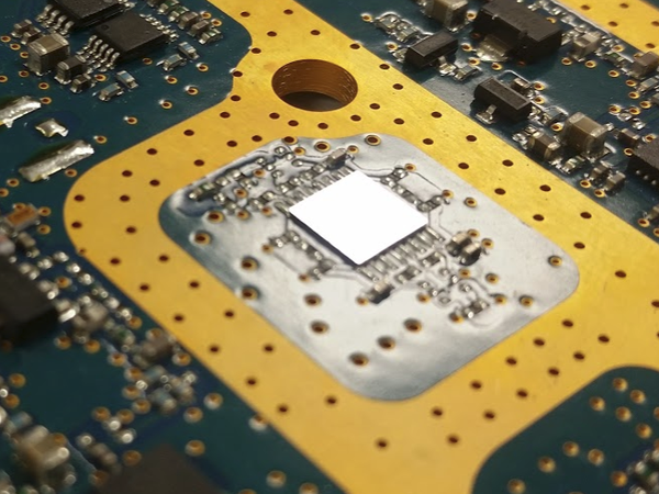
In this application, eight photodiode arrays are placed and soldered on a ceramic circuit carrier. In the manufacturing process, some of these chips fail or do not meet the requirements and therefore need to be replaced.
The application includes the following process steps:
- Desoldering of the faulty photodiode array.
- Full removal of the residual solder from the circuit carrier.
- Uniform wetting of the chip’s contacts with flux and high-precision placement on the circuit carrier using a flip-chip method.
- Soldering of the chip on the circuit carrier in a defined position.
The main challenges are:
- The ceramic circuit carriers are populated from edge to edge. A secure method for fixing the circuit carrier in the rework system had to be developed.
- The distance between the sensors (which are soldered in two rows of four) is only a few micrometers. However, adjacent chips may not be melted, touched or moved during desoldering, placement and residual solder removal. This imposes special requirements on the tools being used.
- To ensure image quality in the CT device, all pixels must be in their correct x/y position. The position of the chips in the z-plane is also crucial, as further functional layers are later bonded to the photodiodes. If all sensors are not plane-parallel to each other, this results in adhesive layers of different thicknesses, which impairs the performance of the CT detector. The tolerance range here is less than 20 micron.
- Silicon sensors have a highly reflective surface and are transparent for wavelengths in the infrared spectrum. This rules out the use of simple IR heaters and more advanced heating technologies must be used instead.
Adapted Solutions for Each Process Step
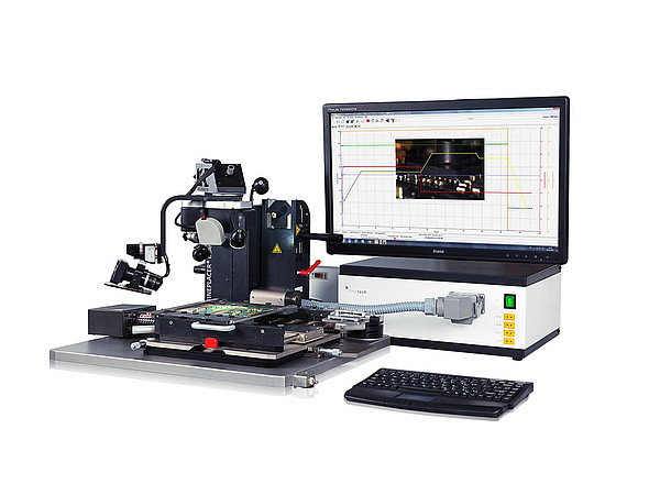
As the ceramic circuit carriers are populated from edge to edge, it was not possible to clamp them into the rework system like a conventional PCB using the positioning table’s clamping rails. Instead, Finetech built a special substrate holder into which the ceramic substrate can be inserted and fixed by vacuum.
Finetech has long-standing experience in the development of customized soldering tools. Adapted tool designs ensure safe rework processes even under very demanding conditions. Finetech was able to quickly design a suitable soldering head for the First sensor application and, in combination with suitable temperature profiles, to set up a reproducible desoldering process.
Thanks to a solder removal module integrated in the rework system, all of the residual solder can be removed by contactless extraction. The special design of the used solder removal head allows the entire surface of the solder joint to be cleaned in a single pass, and at the same time reliably protects neighboring chips from melting and shifting.
Prior to placement, the solder balls of the replacement sensor are wetted with flux and Finetech’s specially manufactured dipping trays proved to be an efficient solution. The contacts of the chip are immersed in a flux bath at a defined depth to ensure a uniform coating of the material on all solder balls.
For the soldering of the new chip, a thermode soldering head was specially designed, which rests on the surrounding sensors during soldering and thereby places the chip at a defined distance on the circuit carrier. In order to ensure co-planarity, the thermode soldering head on the system’s soldering arm is precisely aligned to the surface of the substrate holder. With the help of laser scanning microscopy, the soldering head design was perfected to the point that placement and soldering results could be achieved within the tolerance range for all chip positions on the carrier (e.g. chip in the middle, chip in edge position).
Prior to the purchase of the machine, the entire rework process was tested, qualified and approved by First Sensor and the end customer in Finetech’s laboratory. The controlling thermocouples of the heating systems are permanently installed and do not rely on a mechanical contact to the component or circuit carrier, which would not have been possible in this application. This ensures that the temperature profiles and therefore the qualified rework process can be reproducibly repeated.
Quick Return on Invest
Finetech’s all-in-one solution impressed the First Sensor representatives and they gave the go-ahead for the purchase of a Finetech rework system. In combination with process modules, tools and temperature profiles tailored to the requirements, it was the key for First Sensor to set up a safe and reproducible rework procedure for faulty photodiode modules, conveniently in the production environment. This saves valuable resources and the Finetech rework system has already paid for itself after a short time.
„When working with Finetech, I was very impressed that we didn’t just receive a machine, but a solution to our problem. This started with the first consultation and extended from the testing and qualification of the process at Finetech to the final acceptance of the machine at our factory.”
Manager Process Technology, First Sensor AG


