At a recent conference, I was approached by two different companies that asked the same question, “what is the smallest die that can be bonded on the Finetech equipment?”.
I had to think back. About two years ago, we worked with a company that had 80µm² die. At the time, the main challenge in bonding this small die was creating a die collet with an extraordinarily small vacuum hole. One of my latest conversations discussed a die that was half the size of the one from two years ago…only 40µm².
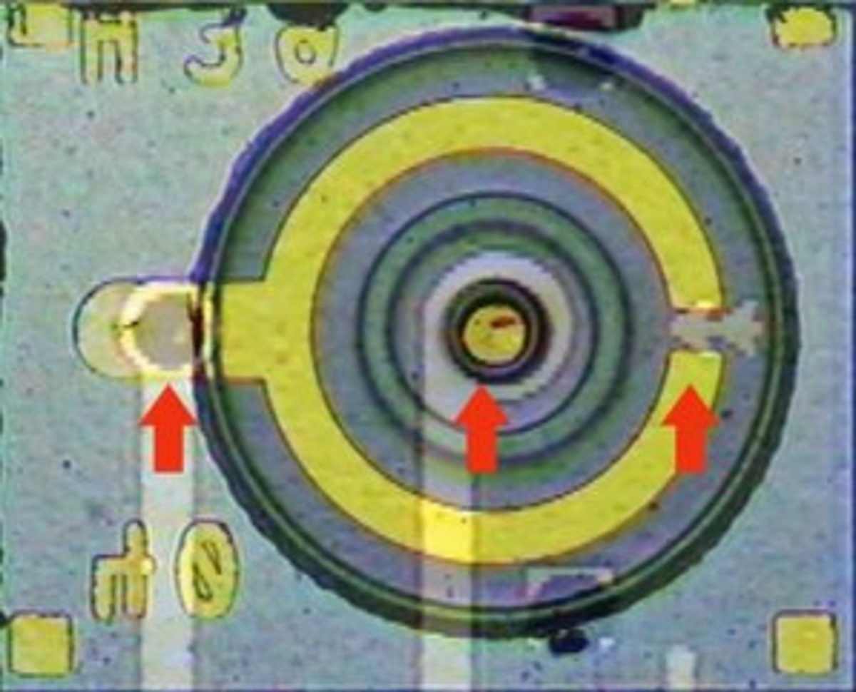
So once again, the tooling challenge came to mind. In addition, optical resolution was a big part of the discussion. If the equipment can’t resolve an extremely small die, then the process stops there (if we cannot see it, we cannot bond it). Apparently, other bonding equipment vendors who claim to have sub-micron accuracy could not view the chip with enough resolution to distinguish one chip from another. Using our Lambda bonder we were able to very quickly look at the die with our optics. Sure enough, we not only could resolve the image quite nicely, we could also say with a high degree of confidence that we could resolve much smaller die. This is exactly what many customers want to do…..reduce the die size even further.
We expect to see more and more applications where the die will become exponentially smaller, and anticipate working with die sizes less than 20µm². With our technology, I am confident that our optical resolution and accuracy will give us a clear pathway to successfully bond these very small die. Sure, tooling is something we have to be prepared to work through, but our bonding equipment is currently capable of handling and resolving such devices. With our optical resolution capabilities, we are positioned to accommodate the toughest challenges.
03/11/2015, created by: Robert Avila

