MEMS components, short for Micro Electro Mechanical Systems, combine micro-scale mechanical structures with semiconductor electronics on a single chip or within a tightly integrated stack. Unlike conventional ICs, MEMS devices interact directly with the physical world. They sense motion, pressure, sound, light or fluids, or actively move and actuate. This physical interaction makes MEMS both powerful and particularly demanding when it comes to MEMS assembly and MEMS bonding processes.
Today, MEMS are embedded across consumer, industrial and scientific applications. They enable motion sensing in smartphones, wearables and drones, support safety and control functions in automotive and industrial systems, and play a growing role in medical devices, LiDAR and photonics. In many products, from wearables to optical systems, MEMS are invisible, yet essential. In all of these applications, reliable MEMS assembly and die bonding directly influence device performance and lifetime.
Their relevance continues to grow as systems become smarter, smaller and more integrated. More sensing capability is expected without increases in size, power consumption or cost, while performance and reliability requirements continue to rise. As a result, MEMS have moved beyond niche applications and become foundational building blocks of modern integrated systems, placing increasing demands on precision MEMS assembly and packaging technologies.
Trends shaping MEMS assembly today
Several technology trends are reshaping MEMS assembly and MEMS packaging. Integration density is increasing as MEMS are combined with ASICs, optical, RF or microfluidic components in a single package. These heterogeneous stacks require precise electrical, mechanical, optical or fluidic alignment, making MEMS assembly a true multi-physics challenge.
At the same time, MEMS dies are becoming thinner and more fragile. Designs based on membranes, cavities and suspended structures are highly sensitive to bonding force, pressure and contamination. In parallel, wafer-level and panel-level packaging approaches push for higher throughput and lower cost. Together, these trends significantly raise requirements for controlled MEMS die bonding, alignment accuracy and process stability.
Reliability expectations are also increasing as MEMS move into safety-critical and regulated markets. Qualification standards, traceability and long-term stability now carry as much weight as initial performance. In this environment, MEMS assembly is no longer a final mechanical step. It directly affects yield, lifetime behavior and the reliable integration of complex MEMS-based systems.
High-accuracy assembly requirements for MEMS devices
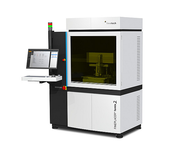
From the perspective of a die bonding solutions provider such as Finetech, MEMS assembly is fundamentally about controlled precision. High-precision die bonding is required to integrate sensitive MEMS devices without introducing mechanical or thermal stress.
Alignment accuracy often needs to reach the sub-micron range, especially when membranes, optical paths or fluidic interfaces must line up precisely. Advanced vision systems must reference complex features such as cavities, apertures or transparent layers, not just die edges or fiducials.
Force control is equally critical in MEMS bonding. Many MEMS components cannot tolerate the bonding forces commonly used in standard semiconductor assembly. Even small deviations can lead to stiction, deformation or latent performance drift. Precise z-control, well-defined bonding force profiles and repeatable process recipes are essential to preserve device integrity.
Thermal management plays a central role as well. MEMS stacks often combine silicon, glass, ceramics and metals with different coefficients of thermal expansion. Uncontrolled temperature profiles during bonding or curing can introduce stress and misalignment. Low-stress die bonding processes and stable thermal control help maintain alignment, yield and long-term reliability.
Cleanliness and surface preparation are decisive factors in MEMS assembly, particularly for cavity-based, optical or near-hermetic devices. Particles, residues or outgassing can compromise performance or cause early failures. Integrated surface treatment, controlled dispensing and monitored curing steps support stable and reproducible MEMS bonding processes.
Beyond precision, production teams increasingly focus on yield and cost. At scale, small variations in alignment, adhesive volume or bonding force quickly translate into yield loss. High-accuracy MEMS assembly is therefore not only a performance requirement, but a direct lever for manufacturing efficiency.
Why customized tooling matters in MEMS assembly
Standard handling and bonding tooling is rarely sufficient for advanced MEMS assembly applications. Customized tooling is often required to protect sensitive structures and ensure stable MEMS bonding processes. This includes tailored clearances for membranes or active zones, venting features to prevent pressure buildup, and compliant tool designs that distribute bonding force evenly across delicate dies.
Tool materials and coatings play an important role as well. Matching thermal expansion behavior, defined compliance and cleanroom-compatible surfaces help reduce stress, contamination and variability. In many MEMS assembly processes, tooling becomes an active element of process control rather than a passive mechanical interface.
Equally important is how tooling integrates into the overall MEMS assembly workflow. Modern MEMS bonding increasingly relies on in-process monitoring, data logging and closed-loop control. Tooling must work seamlessly with vision systems, force sensors and software to support repeatable, qualification-ready MEMS assembly, especially in regulated markets where documentation and traceability are mandatory.

MEMS assembly with customers in development and production
The growing importance of precision MEMS assembly is reflected in many customer projects we support.
In R&D environments, teams developing innovative MEMS sensors rely on flexible die bonding platforms to evaluate different bonding technologies while protecting fragile structures. High alignment accuracy and gentle handling allow early prototypes to behave like future production devices.
In other applications, such as the stacking of large membrane chips, sub-micron post-bond accuracy is required to ensure functional performance. Controlled bonding forces, customized tooling and real-time monitoring enable reproducible results that are difficult to achieve with conventional assembly systems.
In industrial production environments, customers use our high-precision die bonding platforms to support advanced MEMS assembly workflows across multiple device types. The combination of accuracy, process stability and scalability allows MEMS concepts to transition from development into volume manufacturing with confidence.
Meet us at IEEE MEMS 2026 in Salzburg
MEMS technology continues to evolve rapidly, and MEMS assembly remains a key enabler of future devices. We look forward to exchanging perspectives on current challenges and emerging solutions at IEEE MEMS 2026 in Salzburg, Austria, from January 26 to 29.
Visit us at Booth 17 to explore how our high-accuracy die bonding systems, customized tooling designs and controlled, repeatable processes form the foundation for robust MEMS assembly workflows.