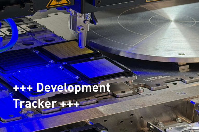

What decides whether an infrared sensor, a quantum processor or a microLED display makes it into production? In advanced packaging, it increasingly comes down to one connection: the indium bump interconnect (IBI) between two chips.
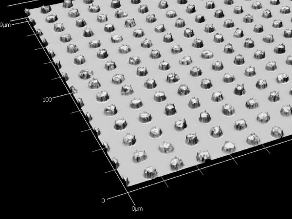
That connection is nearly identical in all three: a fine-pitch array of micro indium bumps, flip-chip bonded, thousands to millions of them across one component. Indium bump interconnect carries the signal in IR focal plane arrays, superconducting quantum processors and the newest microLED displays. In each case the bond is now harder to make than the chip it connects.
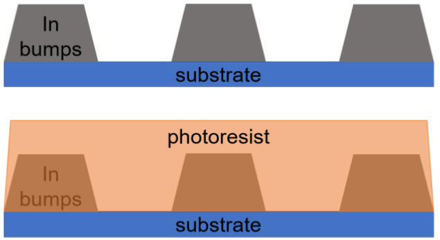
When it fails, the failure is specific: a qubit that loses coherence, a dead pixel on a sensor, a blind spot on a display. Three products, one root cause at the bond interface.
In advanced packaging, the assembly has become the bottleneck, not the chip. The device is only as good as the bond that connects it, and whoever masters that connection once holds a piece of all three markets.
Finetech has spent years turning IBI flip-chip bonding into a single standardized process that holds across all three, rather than a set of tricks retuned for each job. Learn why indium bump interconnect flip chip bonding has become so decisive and download our whitepaper for full process details.
Indium Is the Only Material That Works, and That Is the Problem
Indium earns its place for reasons the alternatives cannot match: it stays ductile at cryogenic temperatures, carries signal with low microwave loss, and flexes to absorb the stress between materials that expand at different rates.
The trouble is scale. Heterogeneous integration keeps pushing pixel and qubit counts up, chips larger, and bump pitch smaller.
IR focal plane arrays are heading toward 20 to 50 mm components covered almost entirely in 5 to 7 µm indium bumps at a 15 µm pitch, leaving a bond line just 2 to 4 µm thick over the whole part. A micron of misalignment or tilt is enough to compromise the array.
The materials rule out the shortcuts. Sensitive structures and mismatched thermal expansion mean these bonds can no longer be forced with high-temperature reflow or formic acid processing. They have to be made cleanly, cold or near-cold, at sub-micron accuracy, and repeatably. That exceeds what most die bonders can hold.
Five Things That Decide Every Bond
Across all three applications, the requirement is the same:
- Sub-micron placement accuracy and co-planarity across the whole component
- A force window narrow enough to bond without deforming the bump
- Handling that keeps the parts clean before bonding even starts
- A clean, oxide-free surface at the moment of placement
- In-process measurement to catch problems on the bonder
Meeting that means controlling every step around the bond, not any single feature. Each of the five below maps to one of these.
Placement and co-planarity are non-negotiable. In the plane, every bump has to land within a fraction of a micron of its target. In height, the array is only microns tall across a component tens of millimeters wide, so tool and substrate have to sit almost perfectly parallel. Sub-micron placement puts each bump where it belongs; passive levelling keeps compression even across the whole part instead of crushing one corner and leaving the other open.

Force control protects what it bonds. The force window is narrow, and controlled ramps at touchdown prevent the sliding and shearing that smear a fine-pitch array. MicroLED runs at the lowest forces of all, to spare far smaller emitters. Quantum adds tight temperature control alongside force, since both affect qubit coherence.
Handling protects yield before bonding even starts. Manual tweezer handling is a main source of contamination and damage, and it matters most where the parts are most fragile, from delicate IR arrays to ultra-small microLED emitters. Dedicated material kitting packs enable tweezer-free loading, handling and flipping, so assemblies move through preparation and bonding with little or no operator contact. This upstream preparation is often where yield is quietly won or lost.
Surface prep decides the bond before any force is applied. Oxide or residue causes voids and weak joints, and it forms the moment a clean surface meets air. An integrated atmospheric plasma step cleans and activates the surface right before placement, with no transfer to a separate tool. Quantum work adds a controlled nitrogen or formic acid environment to keep indium interfaces oxide-free. The same principle protects sub-micron microLED bonds from the contamination that would show up as dead pixels.
In-situ measurement closes the loop. A laser height sensor maps flatness, checks co-planarity and estimates bond line thickness on the bonder, catching problems there instead of downstream.
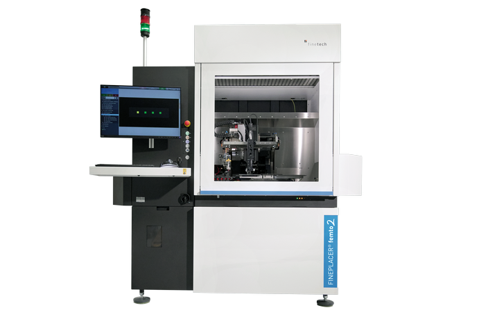
None of these steps is exotic alone. The difficulty is holding all of them together, repeatably, across a component almost entirely covered in interconnects. That is what Finetech has standardized into a single IBI flip-chip process on the FINEPLACER® femto 2.
The Same Bond Under Three Very Different Chips
The same standardized IBI process carries across three very different markets. Each values it for a different reason, but the achievement is the same: a repeatable, high-yield bond that moves from R&D into production.
IR sensor assembly. For infrared focal plane arrays, a rapid, protected path from R&D to high-yield production.
- Interconnect yield above 99% on real FPAs, through functional and cryogenic stress testing
- First sample to a successful bond in as little as six hours
- Standardized tooling and minimal, non-sensitive product data, so IP stays in-house
Learn more about Finetech’s IR sensor assembly fast-track approach
Quantum packaging. For superconducting quantum processors, the same process enables 3D integration, connecting stacked qubits to control and readout electronics through superconducting indium interconnects.
- Sub-micron placement and sub-1 µm co-planarity, with interconnect yields above 99%
- Force and temperature control fine enough to protect qubit coherence, stable under repeated cryogenic cycling at millikelvin temperatures
- From concept to a scalable, error-protected architecture for fault-tolerant QPUs
Learn how Peak Quantum is building fault-tolerant superconducting qubits.
MicroLED assembly. For next-generation microLEDs, indium bump flip-chip bonding carries the sub-micron precision the smallest emitters need.
- Cold compression bonding of emitters as small as 300 nm, at ultra-low force and room temperature
- Sub-micron flatness and co-planarity, so even the smallest emitters contact uniformly
- Initial yield above 85%, from lab into pilot production
Read more on how Polar Light Technologies is developing the next generation of MicroLED displays.
The Thousandth Bond Has To Match the First
Each of these stories turns on repeatability. A single good bond in development shows the process can work. Holding that result across thousands of cycles shows it can go into production.
- An IR sensor assembly process that hits sub-micron accuracy once means little if it drifts by the next duty cycle
- A quantum integration that works on a demonstrator still has to survive the handoff to a line
- A microLED yield above 85% matters only if batch bonding holds that precision
What counts is how little accuracy and yield move across days, shifts and operators.
Scaling IBI is therefore as much about automation as accuracy: the same sub-micron process has to become more automated and less operator-dependent as volumes grow, without loosening its tolerances. Automated handling, calibration and measurement point that way, and support for substrates up to 12-inch wafers is part of carrying that precision into higher-volume production.
The Bond Only Gets Harder From Here
The direction of travel is set: smaller bumps, bigger components, higher density, and rising cost pressure as wafer-level approaches sharpen the focus on cost per bond. Every one of those trends makes the bond harder and process control more decisive.
IR thermal imaging, quantum computing and microLED will keep looking like separate industries, but underneath they converge on one requirement: place more interconnects, more accurately, at higher yield, and hold it in production. That is how much of a strategic core process IBI has become, and why mastering it at scale is now decisive for whether many devices reach production at all.
Want to see how the process runs? Our whitepaper goes deeper into levelling and force windows, bond force and temperature profiles, the co-planarity and accuracy methodology, and the reproducible process parameters behind the results here.